


AUTO & AV Chip Data Sheet
Features
- Glass Passivation Junction
- Low Forward Voltage Drop
- High Current Capability
- High Reliability
- High Surge Current Capability
- Compatible With Soldering
- Surface Metalization:Ni/Au
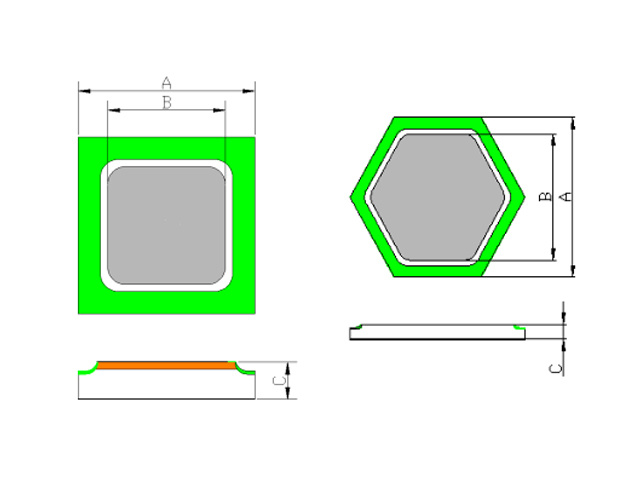
Dimensions
|
Chip size |
A (+1/-2)(mil) |
B(+1/-2)(mil) |
C(±10) |
|
Square |
|
|
|
|
180*180mil |
180 |
155 |
205 |
|
200*200mil |
200 |
176 |
205 |
|
215*215mil |
215 |
191 |
205 |
|
220*220mil |
220 |
196 |
205 |
|
Hexagon |
|
|
|
|
220*220*220mil |
220 |
198 |
205 |
|
240*240*240mil |
240 |
218 |
205 |
Electrical Characteristics (TA=25℃)
|
Parameter |
Symbol |
VALUE |
UNIT |
|
Maximum repetitive peak reverse voltage |
VRRM |
400 for AUTO only |
V |
|
Maximum RMS voltage |
VRMS |
300 for AUTO only |
V |
|
Maximum DC blocking voltage |
VDC |
400 for AUTO only |
V |
|
Maximum average forward rectified current |
IF(AV) |
See Next Table |
A |
|
Maximum instantaneous forwad voltage at IF |
VF |
See Next Table |
V |
|
Peak forward surge current 8.3 ms single half sine-wave superimposed on rated load |
IFSM |
See Next Table |
A |
|
Maximum DC reverse currentat rated DC blocking voltage |
IR |
See Next Table |
uA |
|
Maximum reverse recovery time. Test conditions:IF=0.5A, IR=1A, IRR=0.25A. |
Trr |
See Next Table |
ns |
|
Operating tempeterature range |
Tj |
-55~150 |
℃ |
Message
If you are interested in our products, please leave your phone number.
Contact Us
Telephone:0571-86698096
Address: Liming Community, Heshun Village, Jingjiang Street, Xiaoshan District, Hangzhou City, Zhejiang Province
E-mail:sales@hzhangxin.com
COOKIES
Our website uses cookies and similar technologies to personalize the advertising shown to you and to help you get the best experience on our website. For more information, see our Privacy & Cookie Policy
COOKIES
Our website uses cookies and similar technologies to personalize the advertising shown to you and to help you get the best experience on our website. For more information, see our Privacy & Cookie Policy
These cookies are necessary for basic functions such as payment. Standard cookies cannot be turned off and do not store any of your information.
These cookies collect information, such as how many people are using our site or which pages are popular, to help us improve the customer experience. Turning these cookies off will mean we can't collect information to improve your experience.
These cookies enable the website to provide enhanced functionality and personalization. They may be set by us or by third-party providers whose services we have added to our pages. If you do not allow these cookies, some or all of these services may not function properly.
These cookies help us understand what you are interested in so that we can show you relevant advertising on other websites. Turning these cookies off will mean we are unable to show you any personalized advertising.
Copyright©2024 SaiJing Electronics Company Limited All Rights ReservedSEO Business License